Nvidia vs Google AI Chips: The Ultimate Battle for AI Dominance (GPU vs. TPU)
⚔️ Introduction: The Core of the AI Chip War
The foundation of today’s artificial intelligence boom—from advanced Large Language Models (LLMs) like GPT-4 and Gemini to groundbreaking scientific research—rests entirely on specialized processing hardware. For years, Nvidia’s GPUs have been the undisputed champions, but a powerful challenger has emerged from within the hyperscaler ranks: Google’s Tensor Processing Units (TPUs). This is the **AI chip war**, a multi-billion dollar contest defining the future of cloud computing and machine learning development. Choosing the right **AI accelerator**—GPU or TPU—is the single most critical decision for any company scaling its AI strategy.
II. Nvidia’s Dominance: The CUDA Moat and GPU Versatility
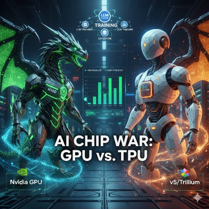
Nvidia commands over 90% of the market for **AI chips**, a lead built on more than just powerful hardware like the **H100 GPU** and the upcoming **Blackwell B200**.
A. The CUDA Ecosystem: Nvidia’s Strategic Advantage
Nvidia’s greatest asset isn’t silicon, it’s **CUDA**. This proprietary software platform, which facilitates parallel computing on Nvidia GPUs, is a powerful “software moat” that locks in developers.
- Broad Adoption: Researchers have been using CUDA for over a decade, resulting in a vast library of optimized code and tools.
- Flexibility: Nvidia GPUs are **general-purpose accelerators**. They can handle training, inference, graphics rendering, and High-Performance Computing (HPC) with equal proficiency, making them the default, safest choice for enterprises with diverse computing needs.
B. The Cutting Edge: H100 and Blackwell B200
Nvidia continually pushes the boundaries of raw single-chip performance. The **H100 Hopper GPU** is the industry standard for high-end **LLM training**. Looking ahead, the **Nvidia Blackwell (B200)** architecture, coupled with the **Grace Blackwell (GB200) Superchip**, promises massive leaps in compute and memory capacity, targeting trillions of parameters and drastically improving inference efficiency through new data formats like FP4.
III. Google’s Challenge: TPUs—Efficiency Through Vertical Integration
Google’s response to the GPU hegemony is the **Tensor Processing Unit (TPU)**. Unlike a general-purpose GPU, the TPU is an **Application-Specific Integrated Circuit (ASIC)**, designed *only* for the matrix multiplication that powers deep learning.
A. Architecture and Cost Efficiency
Google TPUs are built for one thing: running Google’s machine learning frameworks (TensorFlow and JAX) with maximum efficiency.
- Performance-Per-Watt: TPUs consistently demonstrate superior **performance-per-watt** and **performance-per-dollar** compared to high-end GPUs for Google’s internal workloads.
- Cloud Focus: TPUs are primarily offered via **Google Cloud Platform (GCP)**. By controlling the entire stack—hardware design, compiler, and cloud environment—Google achieves optimization impossible for third-party vendors.
- Scaling Pods: Google’s custom **Inter-Chip Interconnect (ICI)** allows them to link thousands of chips into massive **TPU pods** (like the v5p), necessary for training models like Gemini.
B. The Next Step: Trillium (TPU v6)
The upcoming **Google Trillium (TPU v6)** is set to double the high-bandwidth memory (HBM) and increase the peak compute performance by up to 4.7X compared to its predecessor. The strategic goal of Trillium is clear: **establish the lowest cost-per-training-token** in the industry, making it the most economical choice for training the next generation of vast foundation models.
IV. Performance and Pricing Comparison: GPU vs. TPU
The true metric of success in the **AI chip war** is the **Total Cost of Ownership (TCO)** for specific AI workloads.
| Feature | Nvidia H100/Blackwell | Google TPU v5p/Trillium | Best For |
|---|---|---|---|
| Workload | General AI, HPC, Graphics | Tensor-Based Machine Learning | Flexibility |
| Cost Per Training Token | High Premium Price | Lower Cost/Token (Estimated) | Cost-Efficiency |
| Inference Efficiency | Excellent with FP4/sparsity support | Optimized for Batch Throughput | High-Volume Serving |
| Availability | All Clouds (AWS, Azure, GCP, On-Prem) | Google Cloud Platform Only | Market Reach |
Key Insight: While the **Nvidia H100** might offer the fastest single-chip performance, the **TPU v5p** is designed to achieve faster, more cost-effective training *at the scale* of multi-thousand chip clusters. For massive companies like Meta and Google, the efficiency gains translate into billions of dollars in savings.
